Design of an Anechoic Chamber for W-Band and mmWave


1
Instituto de Telecomunicações, 3810-193 Aveiro, Portugal
2
Instituto Superior de Engenharia de Lisboa, 1959-007 Lisboa, Portugal
3
Instituto de Engenharia de Sistemas e Computadores, Tecnologia e Ciência, Faculdade de Engenharia da Universidade do Porto, 4200-465 Porto, Portugal
*
Author to whom correspondence should be addressed.
†
These authors contributed equally to this work.
Electronics 2020, 9(5), 804; https://doi.org/10.3390/electronics9050804
Submission received: 27 April 2020
/
Accepted: 8 May 2020
/
Published: 13 May 2020
(This article belongs to the Section Microwave and Wireless Communications)
Abstract
:In this paper, we describe the design of an electrically large anechoic chamber for usage on millimetre-wave bands. Ansys Savant sotware was used to perform a simulation of the chamber, using physical optics coupled with uniform theory of diffraction (PO/UTD). Moreover, a method based on an open waveguide probe is described in this paper to obtain the electrical properties of the RF absorbers at millimetre-wave frequencies. Two different source antennas were simulated in this work and the corresponding quiet zones predicted. The largest quiet zone was , for a chamber size of .
1. Introduction
The history of wireless communications began around 1895, when Guglielmo Marconi performed the first successful radio communication between two distinct places, demonstrating the transmission of radio signals without wires. Since then, the evolution has been massive and continuous with no limit in sight. In the first decades, wireless signals were used mainly for broadcasting purposes. After that, when Martin Cooper invented the first handheld cellular mobile phone, the mobile communications revolution began.
The first wireless mobile networks were introduced in Japan, Scandinavia and United States in 1979, 1981 and 1983 respectively. This first generation, 1G, of wireless networks was based on a technology called Advanced Mobile Phone System (AMPS), which used analogue signals to enable voice communication. The second generation, 2G, emerged in the 1980s and introduced a new technology with a big success, the Global Systems for Mobile Communication (GSM) and the digital communication was a reality. In 2000, 3G wireless communications introduced video calls and data connection speeds of 0.2 to 2 Mbps. In 2008, 4G wireless communications improved the data rate to 100 Mbps and made available more advanced multimedia services, as well as high-quality video streaming.
The term 5G refers to a variety of technologies that intend to create ultra-fast wireless connectivity, aiming to achieve data rates of 20 Gbps, extremely low latency, and significant improvement in users’ quality of service (QoS), when compared to 4G Long Term Evolution (LTE) networks. 5G networks achieve these higher data rates by using higher frequencies, in or near the millimetre wave band from 30 to 300 GHz. These high frequencies open up a wide spectrum for higher bandwidth channels, that accommodate extremely high speeds. However, these changes imply significantly more base stations than needed when using lower frequencies, because these type of waves tend to be quite short and easily obstructed by even small objects. In order to solve the problem, 5G will require a different architecture, using multiple smaller, low-power microcell base stations, with Massive Multiple Input Multiple Output (MIMO) antennas, which are able to send and receive more data simultaneously, connecting more users at the same time to the network, while maintaining high throughput.
With the introduction of 5G and beyond, the impact on the networks will be severe because a new paradigm is introduced. The changes are not only in the antenna design and measurement process, but also in the used concepts. Now, the user equipment design is based on a distributed phased-arrays architecture [1,2], enabling a multistream multi-beam communication mode, which will enhance the data throughput. Moreover, the move to higher frequency bands in the mm-wave region implies that the antennas have small dimensions, the free path loss is higher and the measurement of the radiation pattern can not be carried out on conventional room-sized anechoic chambers. It is also important to reduce the length of coaxial cables, because at millimetre wave frequencies the losses on these devices are too high. This dictates the need for anechoic chambers specifically designed for operation at these frequencies.
Considering the existing computational capacity, the design of anechoic chambers is nowadays highly supported by electromagnetic simulators, which provide a higher confidence on the final design. In [3], the authors used the ray-tracing method to evaluate the reflectivity level of an anechoic chamber, in the frequency range 100–500 . They also used genetic algorithms to optimize the layout of ferrite tile absorbers in a partially lined enclosure, in order to reduce the cost and simultaneously achieve a better performance. Although this solution was successful for low frequencies, the same was not verified for high frequencies, due to the high reflectivity of the ferrite at those frequencies.
In [4,5] the performance of anechoic chambers at very high and ultra high frequency bands (VHF/UHF) was evaluated based in computational electromagnetic tools. These tools were used to understand the requirements to design and construct a custom anechoic chamber without compromising the performance. Campbell et al. used a finite element method (FEM) simulation at low frequencies, since the electric dimensions of the chamber were small. However, the chamber size was approximately , at , which forced the authors to use PO asymptotic method instead, showing that full wave simulation is infeasible when electrically large structures are considered. Xu et al. employed full wave simulation methods only to one of the absorber pyramids, by using periodic boundary conditions. After obtaining the reflectivity of the absorber, they employed it in a ray tracing based simulator. This approach showed to be a good compromise between simulation complexity and accuracy. Nonetheless, this can only be used when the pyramidal absorbers themselves are electrically small, rendering this technique useless when electrically large absorbers are used. Due to physical limitations, even the smallest absorbers can be electrically large and inadequate for full-wave simulation, which leads us to the only option of using the PO/UTD method.
Wayne et al. presented in [6] the typical metrics (amplitude taper and ripple, phase variation, and cross polarization) used to evaluate the quiet zone quality. It is expected that if the metrics are met, then measurements of an antenna placed within that quiet zone, present low uncertainty. In [7] presented a new concept for an anechoic chamber. A fully metallic ellipsoid chamber is proposed, in which the source antenna is placed in one of the focal points and a spherical absorber is located on the other focal point. In the middle of these two points a quiet zone exists, where the antenna under test can be placed for measuring. However, this geometry presents an obvious challenge in the process of building it.
In order to better understand the implications of using higher frequencies, if the used frequency is 100 GHz, the wavelength is only 3 mm. If we use an array of , the global dimensions of the antenna are only 6 cm×6 cm and for these dimensions and frequencies it is more convenient a compact anechoic chamber to perform the measurements. With this manuscript we don’t pretend to replace the conventional chambers but to present an alternative more convenient for radiation patterns measurements in these frequencies bands. However, the presented design is not only to obtain a smaller chamber but also understand the radio wave absorbers behaviour, the antenna gain and the attention that must exist in order to obtain a credible measurements in these frequency bands.
This change in the antenna paradigm implies that a new anechoic chamber must be redesigned in order to attend the requirements of 5G antennas and beyond. Due to the higher free-space losses at higher frequencies, room sized chambers suffer from large signal attenuations and cable placement problems. In this paper, we present an anechoic chamber design suitable for antenna measurements at millimetre wave range, using PO/UTD simulations, which has never been reported to the extent of the authors’ knowledge. We show how this simulation method can be used to obtain the incident and reflected fields, in an electrically large yet reduced size chamber, with electrically large absorber geometries. Such process was made using two source horn antennas, with different gains, in order to demonstrate the impact of source antenna selection. Finally, by post-processing the field data obtained from the PO/UTD simulation, we could obtain the quiet zone dimensions and its spatial representation.
2. Anechoic Chambers
In the design of wireless communication systems, it is a crucial issue to choose an antenna that meets the system requirements in terms of radiation pattern, directivity, bandwidth and polarization. To perform the study of antennas, an echo free environment is required and for that purpose anechoic chambers are used.
Traditionally, indoor and outdoor measurement methods were used for this kind of study. The outdoor measurements take place in an open test area, which is weather dependent, suffering abundant reflections, interferences and scattering of EM field within the testing zone. On the other hand, indoor measurements are more accurate and require less space. For these type of measurements, a controlled RF quiet or echo free environment is commonly used, and it can be provided by anechoic chambers filled with absorber materials. In 1953 the first commercialization of microwave absorbers started, and in the same year the first anechoic chamber was under investigation to be used for antenna measurements [8]. Before this, absorbers and anechoic chambers were mainly used for military purposes. The biggest progress in anechoic chambers and microwave absorbing materials, was taken in recent years.
An anechoic chamber or anti-echo chamber, can be defined as a chamber developed to reduce unwanted reflected energy, by the use of absorber materials, providing a “virtual” free-space testing chamber. This special room is used to perform a variety of antenna measurements, electromagnetic interference (EMI) measurements, and electromagnetic compatibility (EMC) measurements, while providing minimal interference from external sources.
The attenuation of external and undesired signals that enter the chamber, is achieved by having the outside of the chamber shielded by metal, reflecting the electromagnetic signals. Even, if parasitic signals can enter the chamber by some small gaps, absorbing materials in the inner walls, door, floor or ceiling, are used to greatly attenuate those signals.
The anechoic chambers for antenna measurements at low frequencies (VHF and UHF bands), are typically made with rectangular and tapered designs. The main objective is to illuminate a test zone surrounding the antenna under test, with an electric field that is as uniform as possible and at same time keep multiple reflections to a minimum. In order to improve the performance of an anechoic chamber, [9,10] introduced a new method, which has shown that the test zone performance can be significantly improved, as well as reflectivity as compared to a conventional chamber layout. By designing the shape of the chamber walls along with the layout of the absorbing materials, significant improvement in the test zone performance is achieved when compared to the results obtained in conventional rectangular chambers.
More recently a new metallic parabolic anechoic chamber structure is presented in [11]. By using the proposed structure, a quiet zone with plane wave illumination is obtained and the parabolic chamber can be used for compact range measurements, which is a significant advantage compared to the similar structures [7,12], whilst maintaining the size of the chamber small.
However, the design of anechoic chambers for millimetre wave band is not common because there are several challenges that still need to be solved. A possible approach is presented in [13] and it uses an extrapolation method. In order to apply this method, it is necessary to change the distance between the transmitter and receiver antennas. Thus, the antenna measurement system consists of a mechanical subsystem and a RF subsystem. However, in the millimetre wave frequency range, the coaxial cables introduce an attenuation level that degrades the dynamic range and makes the measurement impossible.
At millimetre wave frequencies the external sources are rare, therefore the shielding of the chamber is optional. However, the structures inside the chamber, including the absorbers, are electrically large, due to the high frequencies under consideration, which significantly impairs the design process and full-wave simulation methods can not be used. Furthermore, the connectivity between the network analyser, the source and antenna-under-test have to be carefully considered, due to the high cost and losses in coaxial cables. In this sense, the design of a chamber for such frequency bands, has to be optimized in order to be just the right size for the desired quiet zone.
3. Radio Wave Absorber Characterization
Radio wave absorbers are the building blocks of anechoic chambers. Their geometry and materials are engineered to provide the absorption of radio waves entering or exiting the anechoic chamber. There are several common types of absorbers, such as pyramidal, wedge, walkway foam absorbers and ferrite tiles. The performance of the selected absorber is determined by the reflection coefficient , which is the relation between the magnitude of reflected and incident electric-fields of plane waves, given by:
Alternatively, the absorber performance can also be described by return loss R in decibels, given by:
The higher the value of R (dB), the better the absorber performance. The reflections from absorbing materials can represent constructive or destructive interference at the receiving antenna, which is typically the antenna under test, therefore they should be minimized.
The main type of absorbers are:
- Urethane Pyramidal Absorber;
- Twisted urethane pyramids;
- Wedge Absorber;
- Ferrite Tiles and Grids;
- Hybrid Absorber.
The absorbers used in this chamber are the Emerson & Cuming WAVASORB VHP-8, which offer a guaranteed reflectivity of for a perpendicularly incident plane wave, in the frequency range of 40–110 . They are available in tiles of pyramids, each one with a height of approximately and a base of . These were readily available from a previous setup and offered a good reflectivity compared to other absorbers in the market. Furthermore, their pyramidal shape and pyramid height result in good absorption characteristics at high incidence angles. Other pyramid heights could be used at the expense of high reflection at larger incidence angles. If we used other absorber suppliers, we would possibly obtain other results in the predicted quiet zone, however it’s important to refer that the absorbers are not the only thing that has impact in the chamber absorption, for example in [7] there are other methods to reduce the absorber usage without implications in the measured results. In conclusion the behavior of the anechoic chamber is dependent of several parameters and not only the absorbers, but it’s obviously important to consider their characteristics.
Despite the good characteristics of the Emerson & Cuming WAVASORB VHP-8 absorbers, no other data such as permittivity, loss tangent and permeability is provided by the manufacturer. Therefore, before employing these absorbers in an EM simulation, their electrical properties have to be determined.
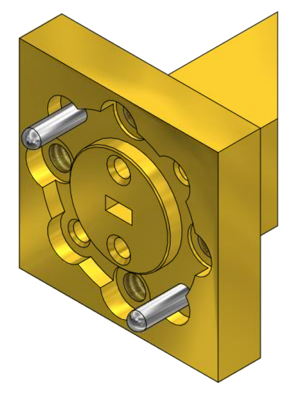
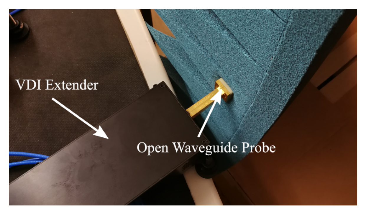
A technique has been widely used for the characterization of lossy dielectric materials, which consists of an open waveguide radiating to a half-space, made of the dielectric under test [14,15,16]. The method is based on measuring the reflection coefficient with the reference plane set in the waveguide aperture and comparing it with the theoretical calculations obtained from modal solutions at the waveguide aperture. However, for mathematical simplicity, the waveguide is usually assumed to have an infinite plane at the aperture plane. According to [17], the waveguide flange can have a significant impact on such methods and effectively introduce measurement errors due to discontinuities. Considering the flange shown in Figure 1, it is expected that significant deviations occur from the theoretical infinite ground-plane approximation, as multiple holes and discontinuities existdue to proper mechanical attachment.
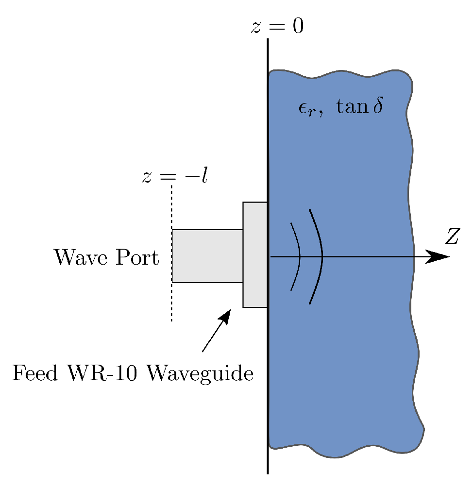
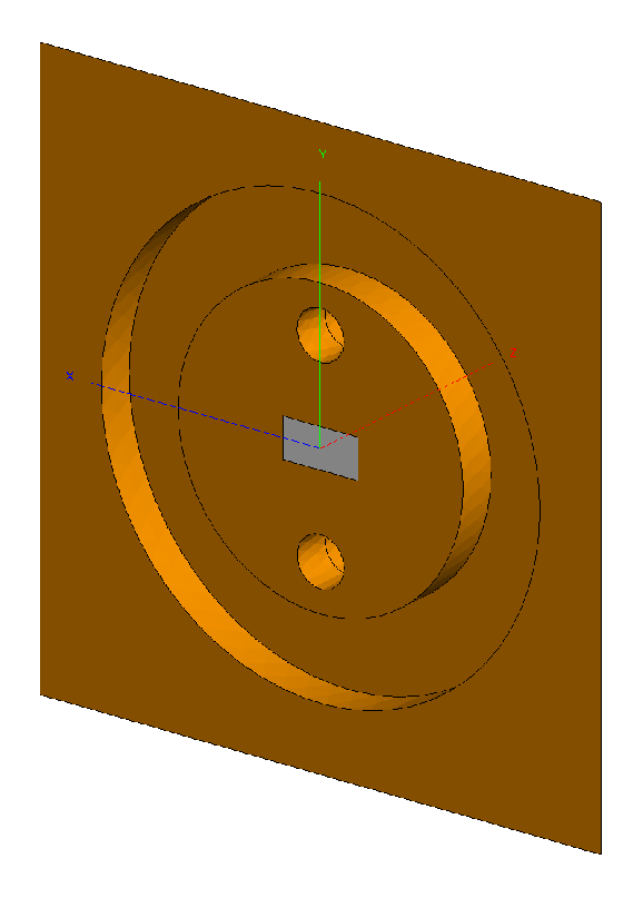
In order to correctly model the behaviour of the physical system, a simulation setup was assembled as schematically shown in Figure 2. The simulation layout of the flange is shown in Figure 3 without the mounting pins. The pins are also removed in the measurement process to avoid punctures in the material under test.
As shown in Figure 2, the reflection coefficient is obtained in simulation, considering a reference plane with an l offset from the desired reference plane located at the waveguide aperture. This occurs because the simulation software does not allow the placement of the wave port directly on the aperture. However, in the measurements using the open-ended waveguide, the reflection coefficient will be obtained at the aperture reference plane, because of the TRL calibration that has to be performed. This offset should be corrected, using the waveguide theory. States, that for a rectangular waveguide we have the factor h defined as
where and are the modal indexes for the mode in which we are operating (TE10). For WR-10 the waveguide width is and its height is . From this point we can calculate the propagation constant of the waveguide as
where is the angular frequency, and are the magnetic permeability and electric permittivity of the waveguide filling medium, which is air in this case. Since the wave at has to propagate to the aperture and back, we can obtain the reflection coefficient of the aperture as
where is the reflection coefficient before the de-embedding process.
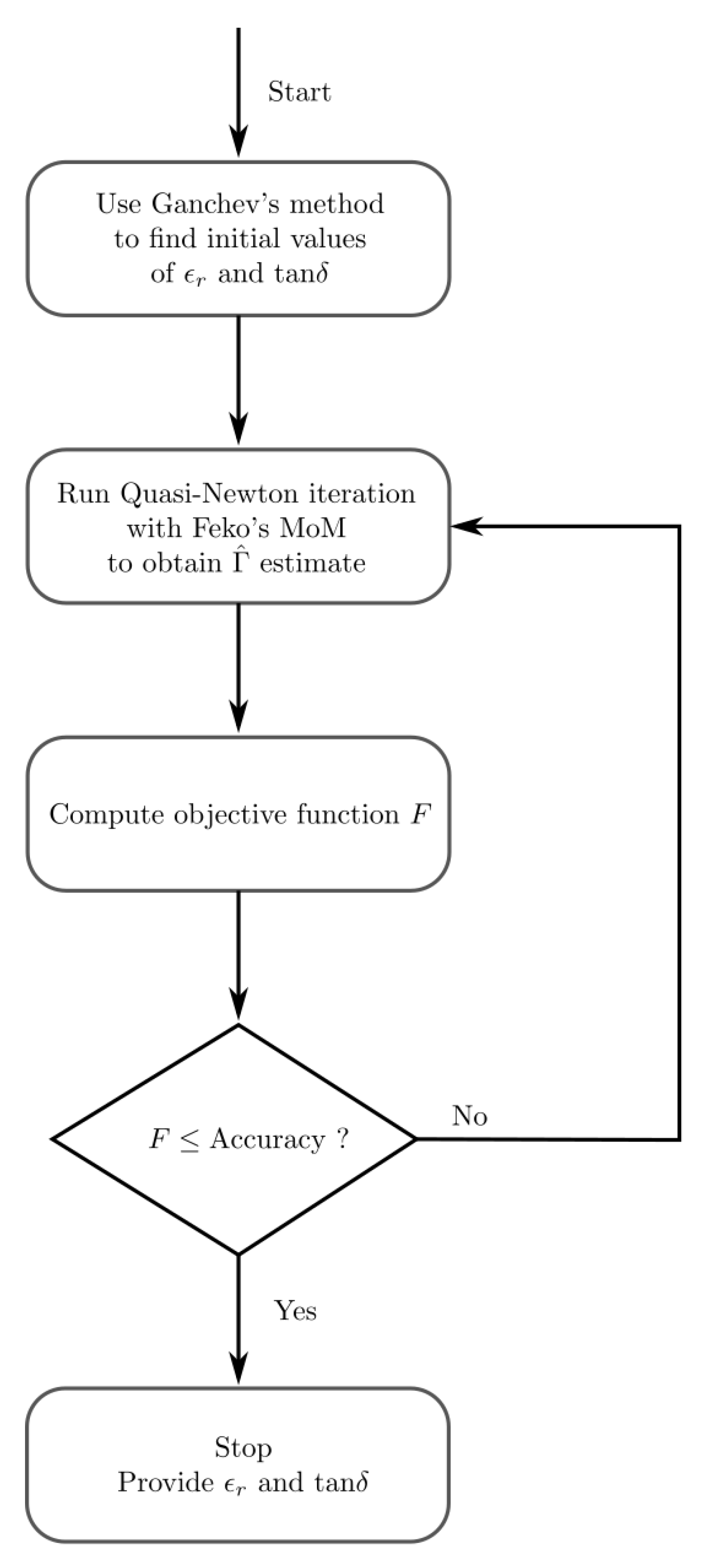
To obtain the dielectric properties of the absorbers, the aperture reflection coefficient must be measured using a VNA, which is represented as . Using this reflection coefficient, the values of and are estimated from the infinite ground plane approximation by using the Ganchev’s method reported in [15]. The absorbers are assumed to be non-magnetic and therefore . Afterwards the retrieved dielectric properties are used as the initial solution for a Quasi-Newton algorithm, whose objective function is
where is the numerically computed reflection coefficient. The properties and are used as tuned variables set in the simulation model of Figure 3, on which a full 3D MoM simulation is run and the estimate of the reflection coefficient is computed. A flowchart representation of the inverse problem resolution by iterative techniques is shown in Figure 4. To obtain the electrical properties of the absorber, the accuracy was set so that when , the algorithm is considered to converge.
4. Chamber Design
Since a plane wave is required at the antenna test zone, the phase variation of the incident wave must be within a specified range. This allow us to define the chamber dimensions that result in a quasi-plane wave to be incident in the antenna test aperture.
According to [19] the curvature of the incident phase front can result in decreased resolution of the antenna measurement process. Considering Figure 6, it is possible to relate the phase differences from the spherical wave to the plane of incidence with . As given in [19] we have
which, if is neglected due to its small value, it results in
Converting the distance of Equation (8) to a phase difference, it yields
The far-field condition is assumed when the phase difference between the radiated spherical wave and a plane wave, is less than [19], which can be equivalently represented as . However, in [19] the authors also show that in the case where the antenna separation is , the nulls of the measured antenna under test (AUT) radiation pattern, deviate significantly from the values that would be obtained in an ideal infinite range. Therefore, to improve the performance of the chamber under design, we employed the criterion of , which approximates better the infinite range condition, with a phase difference of .
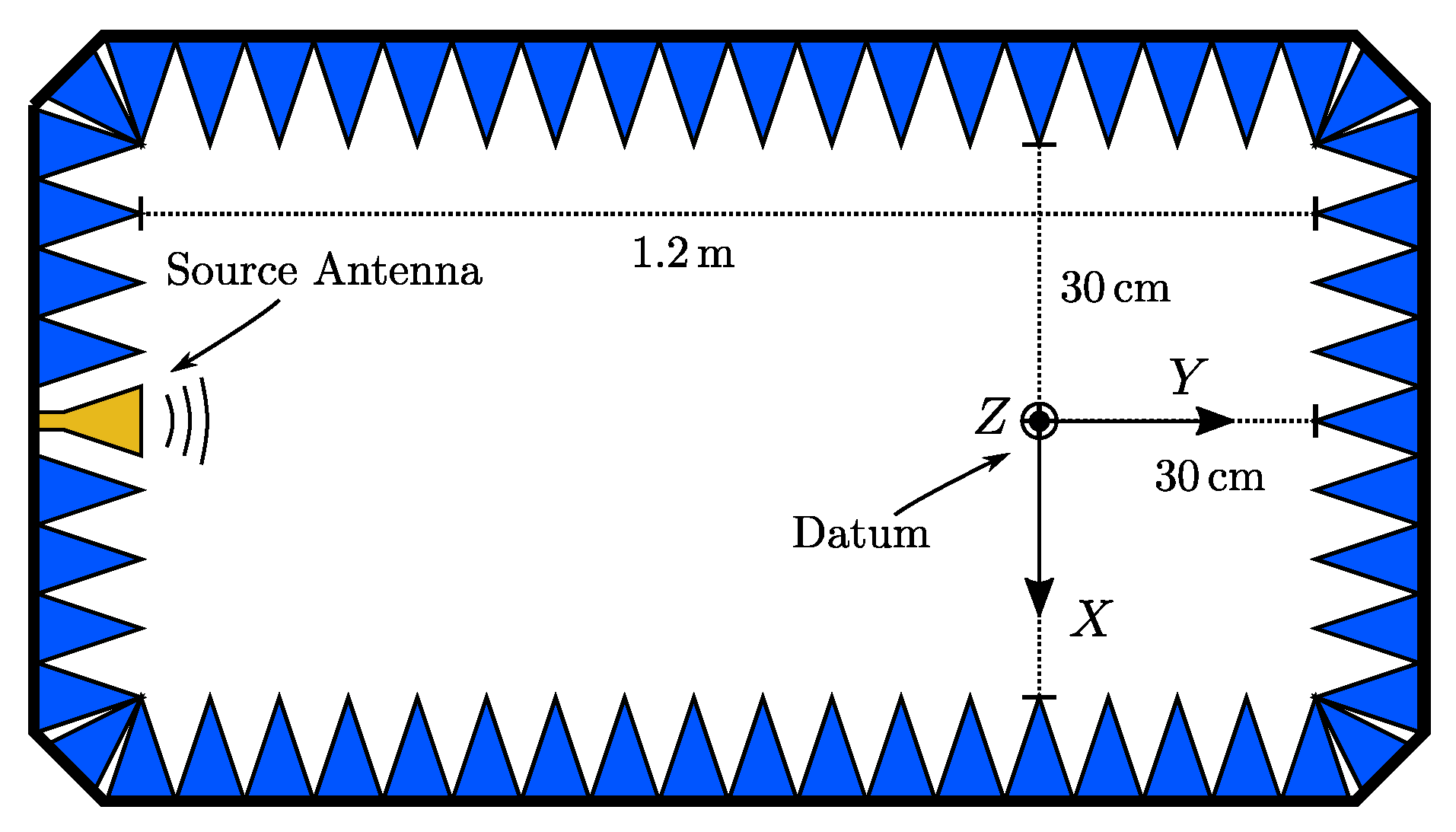
In order to obtain a test aperture diameter of at , which ensures that even moderately large antennas can be tested, the minimum distance of the aperture to the phase centre of the source antenna can be obtained as
Since the absorber tiles are in size, we can use a two tile length chamber, i.e., make the chamber length to be . According to [20], to have an incidence angle less than in the main specular point, the chamber width should be at least , which in our case corresponds to use only one absorber tile. Equivalently, the chamber height was also selected to be equal to the width .
Given these conditions, we designed the chamber to have the required width and length, as shown in the schematic of Figure 7. In the next section we show how we assessed the chamber using PO/UTD simulation in Ansys Savant software to determine its quiet zone.
5. Results
The testing zone of an anechoic chamber must meet a set of requirements for antenna measurements to be feasible. Namely, the incident field phase should be as constant as possible, so that plane wave assumption is valid. This was addressed in the previous section, which led to the specification of the chamber dimensions. Furthermore, the taper of the field amplitude in the test aperture must be below a specified level, which depends on the measurement error that can be tolerated. The reflections coming from the absorbing pyramids result in ripple occurring along the test aperture. This in turn has a direct relation to the amplitude of the field reflected by the absorbers in the chamber [19]. The zone in which all of these requirements are met is called the quiet zone.
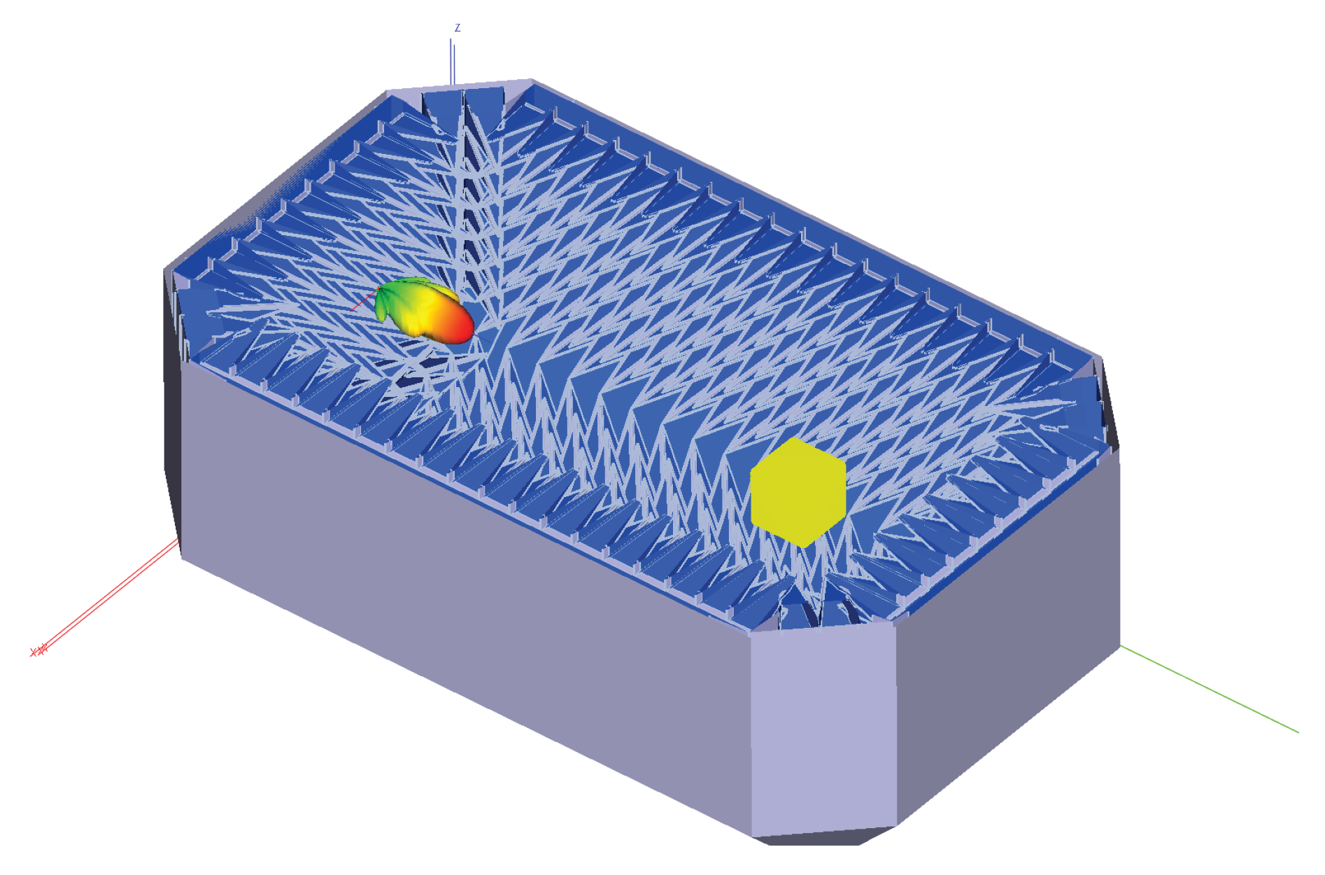
The model shown in Figure 8 was assembled in Ansys Savantsoftware for simulation. The incident and reflected fields represented by the 3D volume in yellow, with and centred on the datum point, are the output of the PO/UTD simulator. This volume allows an acceptable simulation time whilst representing enough space to evaluate the quiet zone location. A limit of two bounces for the rays is defined, which ensures the reduced memory usage and yet enough accuracy, since one ray bounce already resulted in a good agreement between simulation and measurements in [4].
As stated before, three conditions have to be met so that a specific volume is suitable for antenna testing. Such assessment was done by post-processing in MATLAB the resultant fields obtained by the simulator. The phase stability requirement was settled as in Section 4, where only the set of points in which was considered. The field amplitude must be constant along the plane of incidence, so that deviations from the measured and ideal infinite range pattern are minimized. As reported in [19], a field amplitude tapper of less than , produces typical gain deviations of less than , which is satisfactory, and thus this was used as our quantitative requirement. Likewise, the reflections that occur on the absorbers, produce a ripple in the field incident in the test zone, which in turn also results in excessive deviations of the measured radiation pattern. An incident field peak-to-peak ripple of less than was set, which results in reflected fields below the incident fields [19].
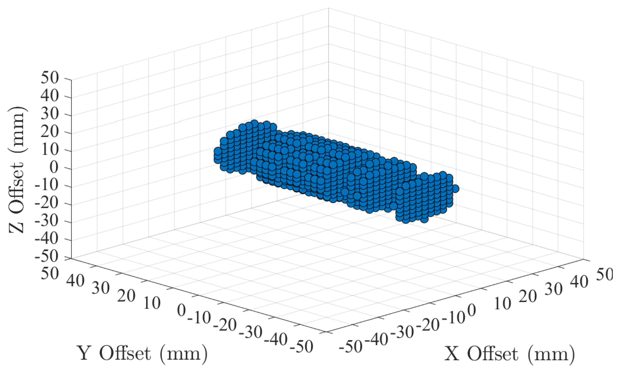
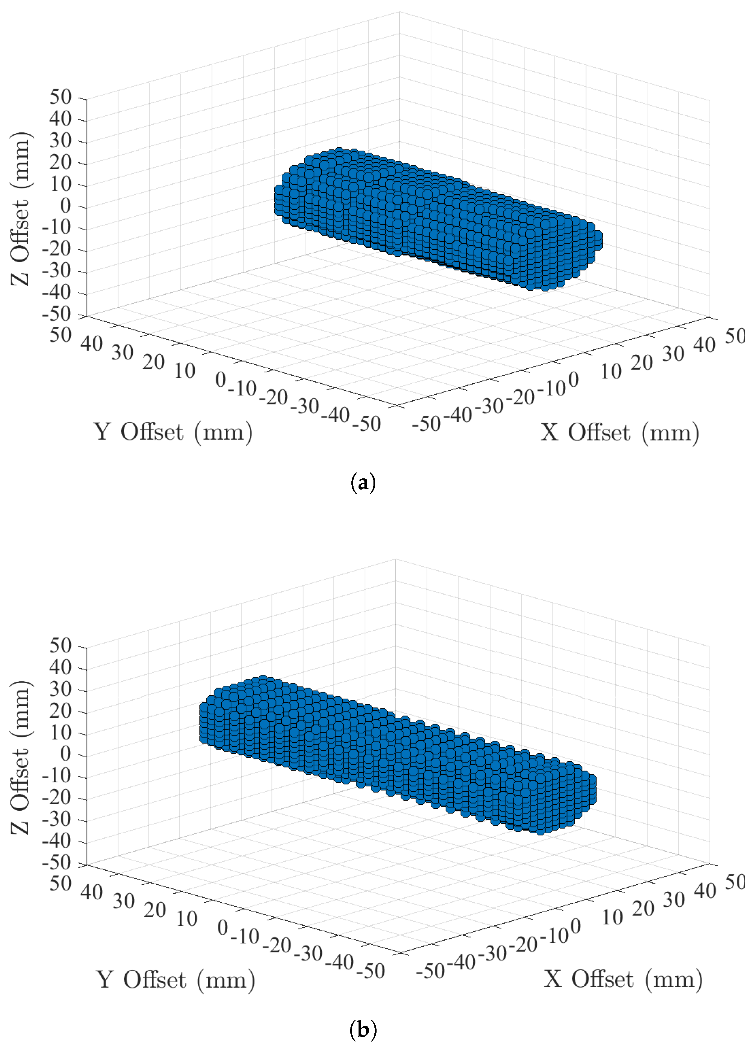
Two simulations for two different source antennas were carried out for three frequencies in W-band, namely 75, 95 and . The first source antenna that was simulated was a horn antenna [21]. The resulting quiet zone at , considering the requirements defined earlier, is plotted in Figure 9, where the origin corresponds to the datum point. No plots are shown for 75 and due to the absence of quiet zone at these frequencies. This allowed us to discard this horn antenna as a source and conclude that due to its beamwidth, the amplitude ripple level was too high. Hence, a second horn antenna with [22] was tested and the resulting quiet zone is shown in Figure 10. In this case, a cylindrically shaped quiet zone was obtained at negative Y offset from the datum. The cylinder has a diameter of approximately and a height of , from the datum in direction to the negative part of the Y axis. Since at 95 and the quiet zones span the whole Y axis, we can infer that is the frequency which defines the quiet zone limitation.
6. Conclusions
In this paper a full design of an electrically large anechoic chamber for millimetre wave was presented. It was verified that the usage of PO/UTD simulation can produce results close to the theoretical expectations and that it can be easily used for evaluating different source antennas, when electrically large absorbers are used. This opens a new ground for the design of anechoic chambers at high frequencies, as in the case of millimetre wave.
The chamber was constructed and in the future some calibrated antennas will be measured to determine the error introduced by our setup.
Author Contributions
Conceptualization, H.S. (Hugo Santos); methodology, H.S. (Hugo Santos) and P.P.; software, H.S. (Hugo Santos); validation, H.S. (Hugo Santos), P.P. and H.S. (Hnrique Salgado); formal analysis, H.S. (Henriquei Salgado); investigation, H.S. (Henrique Salgado); resources, H.S. (Henrique Salgado); data curation, H.S. (Hugo Santos); writing–original draft preparation, H.S. (Hugo Santos) and P.P.; writing–review and editing, H.S. (Henrique Salgado); visualization, H.S. (Hugo Santos); supervision, H.S. (Henrique Salgado); project administration, H.S. (Henrique Salgado); funding acquisition, H.S. (Henrique Salgado). All authors have read and agreed to the published version of the manuscript.
Funding
This work is funded by FCT/MCTES through national funds and when applicable co-funded EU funds under the project UIDB/50008/2020-UIDP/50008/2020.
Conflicts of Interest
The authors declare no conflict of interest.
References
- Huo, Y.; Dong, X.; Xu, W.; Yuen, M. Enabling Multi-Functional 5G and Beyond User Equipment: A Survey and Tutorial. IEEE Access 2019, 7, 116975–117008. [Google Scholar] [CrossRef]
- Huo, Y.; Lu, F.; Wu, F.; Dong, X. Multi-Beam Multi-Stream Communications for 5G and beyond Mobile User Equipment and UAV Proof of Concept Designs. In Proceedings of the 2019 IEEE 90th Vehicular Technology Conference (VTC2019-Fall), Honolulu, HI, USA, 22–25 September 2019; pp. 1–5. [Google Scholar] [CrossRef] [Green Version]
- Razavi, S.M.J.; Khalaj-Amirhosseini, M. Optimization of an anechoic chamber with ray-tracing and genetic algorithms. Prog. Electromagn. Res. 2008, 9, 53–68. [Google Scholar] [CrossRef] [Green Version]
- Campbell, D.; Gampala, G.; Reddy, C.; Winebrand, M.; Aubin, J. Modeling and Analysis of Anechoic Chamber Using CEM Tools. Appl. Comput. Electromagn. Soc. J. 2013, 28, 755–762. [Google Scholar]
- Xu, Q.; Huang, Y.; Zhu, X.; Xing, L.; Duxbury, P.; Noonan, J. A Hybrid FEM-GO Approach to Simulate the NSA in an Anechoic Chamber. Appl. Comput. Electromagn. Soc. J. 2017, 32, 1035–1041. [Google Scholar]
- Wayne, D.; Fordham, J.; McKenna, J. Effects of a Non-Ideal Plane Wave on Compact Range Measurements. In Proceedings of the 36th The Antenna Measurement Techniques Association Annual Meeting Symposium, Tucson, AZ, USA, 12–17 October 2014. [Google Scholar]
- Farahbakhsh, A.; Khalaj-Amirhosseini, M. Using Metallic Ellipsoid Anechoic Chamber to Reduce the Absorber Usage. IEEE Trans. Antennas Propag. 2015, 63, 4229–4232. [Google Scholar] [CrossRef]
- Emerson, W. Electromagnetic wave absorbers and anechoic chambers through the years. IEEE Trans. Antennas Propag. 1973, 21, 484–490. [Google Scholar] [CrossRef]
- Winebrand, M.; Aubin, J.; Boumans, M. A two-Level GTD utilization in designing anechoic chambers for antenna measurements. In Proceedings of the 2009 IEEE Antennas and Propagation Society International Symposium, Charleston, SC, USA, 1–5 June 2009; pp. 1–4. [Google Scholar] [CrossRef]
- Aubin, J.; Winebrand, M. Side wall diffraction optimal back wall design in elongated chambers for far–field antenna measurements at VHF/UHF frequencies. In Proceedings of the 2010 IEEE Antennas and Propagation Society International Symposium, Toronto, ON, Canada, 11–17 July 2010; pp. 1–4. [Google Scholar] [CrossRef]
- Farahbakhsh, A.; Zarifi, D. Analysis and design of metallic parabolic anechoic chamber. In Proceedings of the 2017 11th European Conference on Antennas and Propagation (EUCAP), Paris, France, 19–24 March 2017; pp. 3053–3056. [Google Scholar] [CrossRef]
- Farahbakhsh, A.; Khalaj-Amirhosseini, M. Metallic spherical anechoic chamber for antenna pattern measurement. Chin. Phys. B 2016, 25, 088401. [Google Scholar] [CrossRef]
- Kang, N.; Kwon, J.; Cho, C.; Park, J. Measurement System for Millimeter-Wave Antennas With Distributed External Local Oscillators and Mixers. IEEE Trans. Instrum. Meas. 2019, 68, 1967–1972. [Google Scholar] [CrossRef]
- Decreton, M.C.; Gardiol, F.E. Simple Nondestructive Method for the Measurement of Complex Permittivity. IEEE Trans. Instrum. Meas. 1974, 23, 434–438. [Google Scholar] [CrossRef]
- Ganchev, S.I.; Bakhtiari, S.; Zoughi, R. A novel numerical technique for dielectric measurement of generally lossy dielectrics. IEEE Trans. Instrum. Meas. 1992, 41, 361–365. [Google Scholar] [CrossRef]
- Bois, K.J.; Benally, A.D.; Zoughi, R. Multimode solution for the reflection properties of an open-ended rectangular waveguide radiating into a dielectric half-space: The forward and inverse problems. IEEE Trans. Instrum. Meas. 1999, 48, 1131–1140. [Google Scholar] [CrossRef]
- Maode, N.; Yong, S.; Jinkui, Y.; Chenpeng, F.; Deming, X. An improved open-ended waveguide measurement technique on parameters ϵr and μr of high-loss materials. IEEE Trans. Instrum. Meas. 1998, 47, 476–481. [Google Scholar] [CrossRef]
- VDI Precision Waveguide Interface; Rev. 2.7; Virginia Diodes, Inc.: Charlottesville, VA, USA, 2014.
- Hollis, J.; Lyon, T. Microwave Antenna Measurements; Scientific-Atlanta: San Jose, CA, USA, 1972. [Google Scholar]
- Chowdhury, N.M.A.; Hossain, S.; Zhao, L.; Liao, Z. Low cost indoor environment for antenna measurement. In Proceedings of the 2008 Canadian Conference on Electrical and Computer Engineeringg, Niagara Falls, ON, Canada, 4–7 May 2008; pp. 001353–001356. [Google Scholar]
- WR-10 Pyramidal Horn Antenna, 20 dBi Gain; Rev. 1.0; SAGE Millimeter, Inc.: Torrance, CA, USA, 2016.
- WR-10 Pyramidal Horn Antenna, 25 dBi Gain; Rev. 1.0; SAGE Millimeter, Inc.: Torrance, CA, USA, 2016.
Figure 1.
VDI waveguide flange [18].
Figure 1.
VDI waveguide flange [18].

Figure 2.
Representation of simulation setup for absorber and characterization.

Figure 3.
Simulation layout of WR-10 flange.

Figure 4.
Flowchart for obtaining and .

Figure 5.
Open waveguide measurement setup of RF absorbers.

Figure 6.
Spherical to plane wave front deviation.

Figure 7.
Chamber design schematic cross section.

Figure 8.
Simulation model used in Ansys Savant software for PO/UTD simulation (top part of the chamber removed for visualization purposes).
Figure 8.
Simulation model used in Ansys Savant software for PO/UTD simulation (top part of the chamber removed for visualization purposes).

Figure 9.
Simulated quiet zone for antenna at .

Figure 10.
Simulated quiet zone for 25 dBi source antenna at (a) 75, (b) 95 and (c) 115 GHz.


Figure 11.
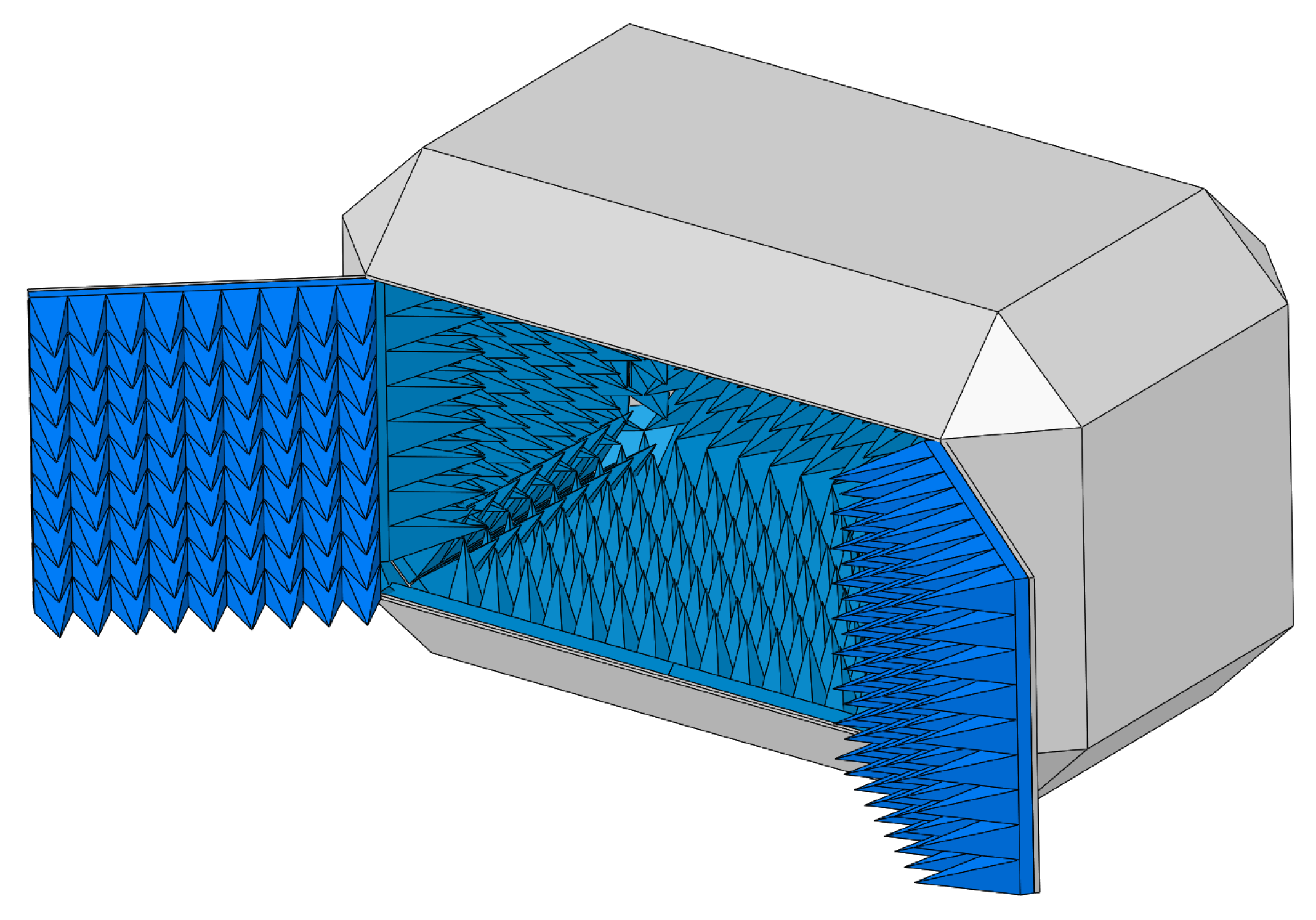
Anechoic chamber 3D design with doors for access to AUT.

Figure 12.
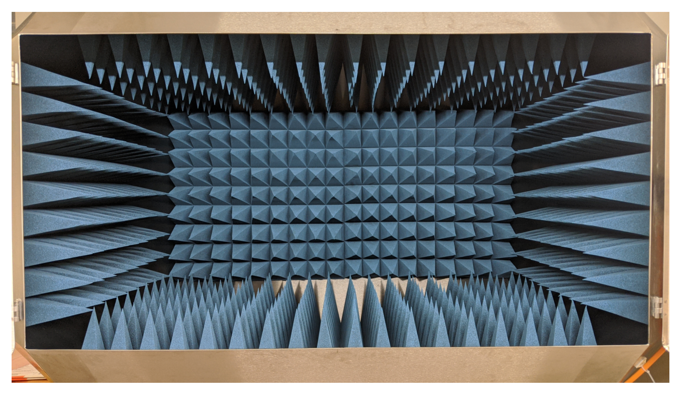
Realized anechoic chamber.


Table 1.
WAVASORB VHP-8 electrical properties at W-band.
| Frequency | |||
|---|---|---|---|
© 2020 by the authors. Licensee MDPI, Basel, Switzerland. This article is an open access article distributed under the terms and conditions of the Creative Commons Attribution (CC BY) license (http://creativecommons.org/licenses/by/4.0/).
Share and Cite
MDPI and ACS Style
Pinho, P.; Santos, H.; Salgado, H. Design of an Anechoic Chamber for W-Band and mmWave. Electronics 2020, 9, 804. https://doi.org/10.3390/electronics9050804
AMA Style
Pinho P, Santos H, Salgado H. Design of an Anechoic Chamber for W-Band and mmWave. Electronics. 2020; 9(5):804. https://doi.org/10.3390/electronics9050804
Chicago/Turabian StylePinho, Pedro, Hugo Santos, and Henrique Salgado. 2020. "Design of an Anechoic Chamber for W-Band and mmWave" Electronics 9, no. 5: 804. https://doi.org/10.3390/electronics9050804
Note that from the first issue of 2016, this journal uses article numbers instead of page numbers. See further details here.